Why Simulation Speed Is Holding Chiplets Back
Multi-physics computational costs are the new bottleneck in advanced semiconductor packaging, directly impacting global supply chains and Malaysia's tech sector.
The semiconductor industry has successfully solved the software toolchain problem for designing heterogeneous chiplets, only to hit a severe hardware bottleneck: simulation speed. Running multi-physics co-simulations across dense 2.5D and 3D chiplet stacks requires immense computational power, driving up costs and slowing down time-to-market. This computational wall restricts the development of advanced artificial intelligence hardware. For Malaysia, a critical hub in the global semiconductor supply chain centered in Penang and Selangor, this constraint directly affects local outsourced semiconductor assembly and test (OSAT) providers and design houses looking to move up the value chain. Overcoming this barrier requires heavy investment in high-performance computing and the adoption of agentic AI to automate and optimize engineering workflows.
AI Summary
The semiconductor industry has successfully solved the software toolchain problem for designing heterogeneous chiplets, only to hit a severe hardware bottleneck: simulation speed. Running multi-physics co-simulations across dense 2.5D and 3D chiplet stacks requires immense computational power, driving up costs and slowing down time-to-market. This computational wall restricts the development of advanced artificial intelligence hardware. For Malaysia, a critical hub in the global semiconductor supply chain centered in Penang and Selangor, this constraint directly affects local outsourced semiconductor assembly and test (OSAT) providers and design houses looking to move up the value chain. Overcoming this barrier requires heavy investment in high-performance computing and the adoption of agentic AI to automate and optimize engineering workflows.
Key Takeaways
- Software toolchains are no longer the primary limit in chiplet design; the massive computational cost of testing them is the new roadblock.
- Multi-physics co-simulation—testing electrical, thermal, and mechanical properties simultaneously—is mathematically and computationally heavy.
- Extended simulation times delay product launches and inflate research and development costs for advanced AI chips.
- Malaysian semiconductor firms must upgrade their high-performance computing infrastructure to remain competitive in advanced 2.5D and 3D packaging.
- Agentic AI systems offer a practical way to manage simulation queues, optimize parameters, and reduce wasted engineering hours.
What Happened
The semiconductor sector has shifted its manufacturing approach. Instead of building massive, single-piece silicon chips (monolithic dies), the industry is moving toward chiplets. Chiplets are smaller, specialized slices of silicon that are packed closely together into a single package. This approach uses 2.5D architecture, where chiplets sit side-by-side on a silicon interposer, and 3D architecture, where they are stacked vertically.
According to Semiconductor Engineering, the software tools used to design these complex structures have matured. Engineers have the necessary software to map out heterogeneous designs—which means combining different types of chiplets, like a memory chip and a processor, into one package. However, the limiting factor has shifted entirely to simulation speed.
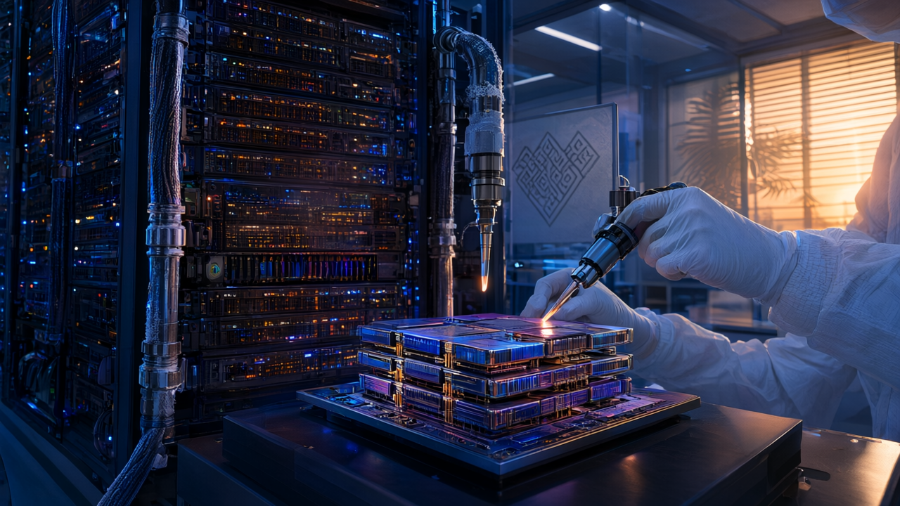
When you pack chiplets this closely together, they generate intense heat, consume massive amounts of power, and face physical stress from thermal expansion. Engineers must run multi-physics co-simulations to see how electrical signals, heat dissipation, and mechanical stress interact simultaneously. Running these combined simulations requires vast amounts of computing power. The computational cost and time required to process these multi-physics equations for advanced 2.5D and 3D stacks have become the primary factor holding back faster chiplet development.
Why It Matters
Time-to-market dictates success in the technology sector. When multi-physics simulations take days or weeks to process, engineers cannot iterate quickly. A design team testing a new cooling solution for a 3D stacked AI processor must wait for the simulation results before physically manufacturing a prototype. This computational bottleneck slows the entire pace of hardware innovation.
This matters deeply because the demand for artificial intelligence infrastructure relies entirely on advanced semiconductors. Generative AI models require immense memory bandwidth and processing power. Chiplets provide a way to scale compute power without hitting the physical limits of single-die manufacturing. If simulation speeds cannot keep pace with design ambitions, the hardware required to run next-generation AI models will face delays and higher production costs.
Furthermore, the financial cost of running these simulations is steep. Design firms must rent massive cloud computing clusters or buy expensive supercomputers just to verify their designs. Smaller design houses risk being priced out of advanced chiplet development because they cannot afford the compute time required to verify their 2.5D and 3D packages.
What This Means for Malaysia
Malaysia holds a critical position in the global semiconductor supply chain, accounting for a significant percentage of global packaging and testing activity. Historically, local operations in Penang, Kulim, and the Klang Valley focused on traditional assembly and test. However, government initiatives under MyDIGITAL and strong foreign direct investment are pushing the country up the value chain into advanced packaging, specifically 2.5D and 3D chiplet integration.
This simulation bottleneck directly affects Malaysian OSATs (Outsourced Semiconductor Assembly and Test providers) and local integrated circuit design houses. As Malaysian facilities transition from traditional wire bonding to advanced wafer-level packaging, they must handle multi-physics complexities for the first time. If local engineers face slow simulation speeds, their yield optimization—the process of ensuring manufactured chips actually work—will suffer.
Malaysian facilities need localized access to high-performance computing to run these multi-physics tests. Relying on cloud servers in the United States or Europe introduces latency, which further slows down the simulation process for local engineers. To secure its position as an ASEAN leader in advanced packaging, Malaysia must build out domestic data center capabilities equipped for semiconductor simulation.
How Your Business Can Use This
If you run a semiconductor design firm or an electronics manufacturing services (EMS) company in Malaysia, you need to re-evaluate your compute budget. Do not just invest in design software licenses. Allocate a significant portion of your capital expenditure to high-performance computing infrastructure, either on-premises or through specialized cloud providers with local regional availability.
For engineering managers, the practical step is to segment your simulation workloads. Run fast, lower-fidelity simulations locally to catch obvious design flaws early. Reserve expensive, high-fidelity multi-physics co-simulations for final verification.
If your business supplies materials, cooling solutions, or testing equipment to semiconductor plants in Penang, you must understand these multi-physics challenges. Your clients are battling thermal and mechanical stress in dense 3D stacks. If you can provide materials with known, predictable thermal properties, you reduce the simulation burden for your clients, making your product more attractive.
The Agentic AI Angle
Autonomous AI agents can directly solve the inefficiencies of multi-physics co-simulation. In a traditional workflow, a human engineer sets up the simulation parameters, hits run, waits for the system to process the data, analyzes the failure points, adjusts the model, and runs it again. This manual loop wastes highly paid engineering hours.
An AI agent can automate this iterative cycle. Using large language models (LLMs) fine-tuned on electronic design automation data, an agent can read the initial thermal data from a failed 3D stack simulation. The agent can then automatically adjust the microfluidic cooling channel parameters in the design file, rewrite the simulation script, and push the job back into the compute queue without human intervention.
The agent acts as a junior engineer, running hundreds of design variations overnight. It filters out the failed designs and presents the human lead engineer with two or three optimized, mathematically sound configurations for final approval. This operationalizes the simulation process, compensating for the raw computational slowness by removing the dead time between simulation runs.
Risks and Limitations
Relying heavily on AI agents to run continuous simulation loops introduces a financial risk. If the agent sets poor parameters, it could burn through thousands of dollars of cloud compute credits overnight without finding a viable design. Human oversight remains critical for setting the boundary conditions of the simulation.
Additionally, data privacy is a major concern. Semiconductor designs represent billions of dollars in intellectual property. Routing sensitive multi-physics design files through third-party cloud servers or external AI agent platforms exposes companies to corporate espionage. Malaysian firms must ensure any agentic AI system runs locally within a secured, air-gapped network or on highly secure private cloud instances compliant with local data regulations.
The Bottom Line
The software tools for designing chiplets are ready, but the computational cost of testing how they physically behave together is slowing down the entire semiconductor industry. Malaysian businesses involved in the electronics supply chain must treat high-performance computing as a core manufacturing asset, not just an IT expense.
This quarter, operations leads at Malaysian semiconductor and EMS firms should audit their simulation infrastructure. Identify where the compute bottlenecks happen during 2.5D and 3D package testing. Begin pilot programs using agentic AI to automate the tedious, repetitive aspects of simulation queuing and parameter adjustment.
FAQ
What is multi-physics co-simulation? It is the process of testing how different physical forces—specifically heat, electrical signals, and mechanical stress—interact with each other simultaneously in a single semiconductor design.
Why are chiplets replacing traditional chips? Building massive single silicon chips is hitting physical and cost limits. Chiplets allow manufacturers to break designs into smaller, cheaper pieces, specialized for different tasks, and pack them closely together to maintain high speed.
How does the simulation bottleneck affect Malaysian tech companies? As Malaysian companies in places like Penang move into advanced semiconductor packaging, they must run these complex simulations. Slow compute speeds delay their design iterations and slow down the entire manufacturing yield optimization process.
Sources / References
- Semiconductor Engineering: Provided the core technical premise regarding toolchain maturity in heterogeneous chiplet design and the identification of multi-physics co-simulation computational costs across 2.5D and 3D stacks as the primary industry bottleneck.
Sources & References
AIBlog summarises and analyses published information. We do not reproduce full source text. Analysis is editorial and not financial or legal advice.