Ultrafast X-Ray Diffraction Maps Thermal Transport In GaN Thin Films (MIT, SLAC, Stanford, Argonne)
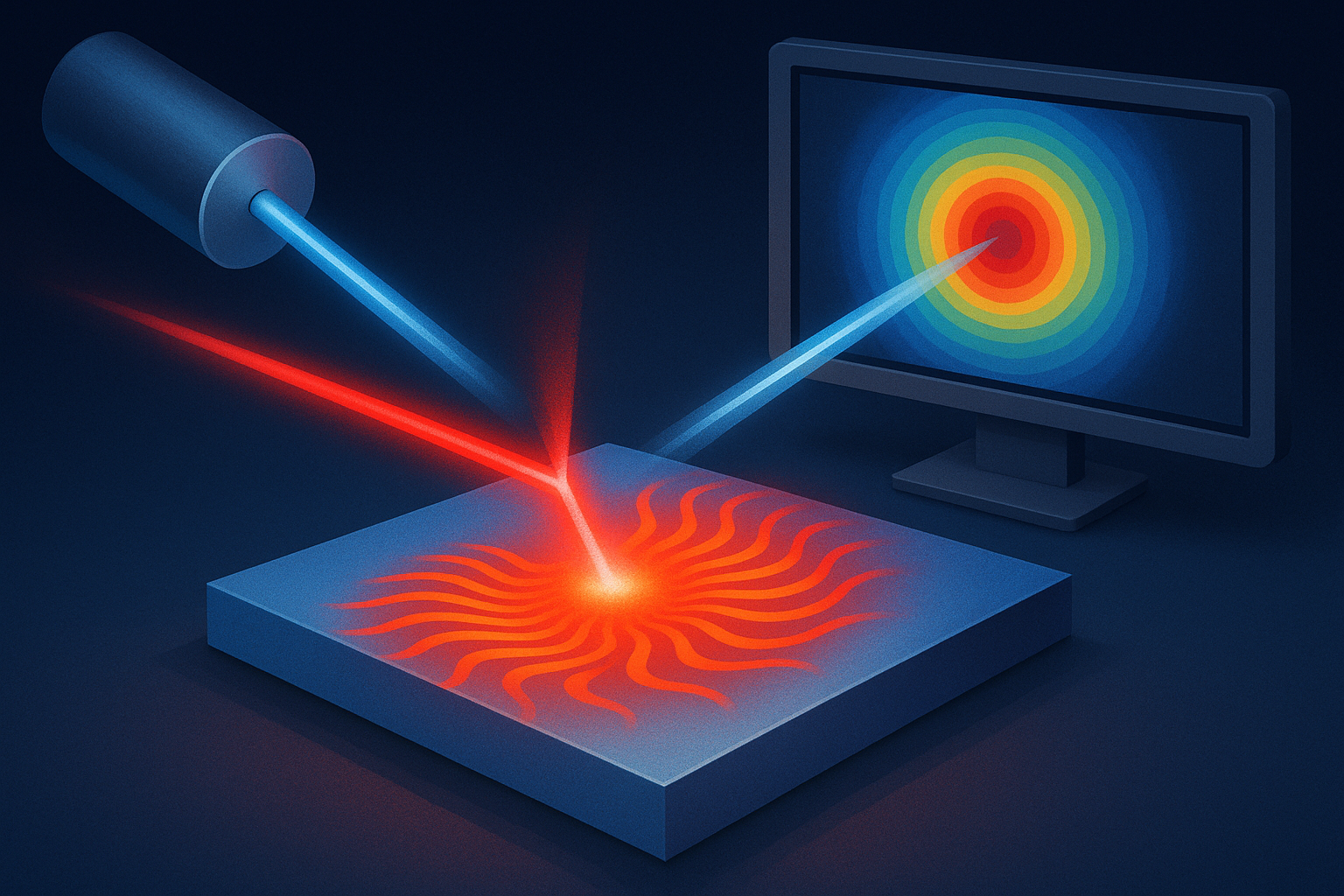
Researchers from MIT, SLAC, Stanford University, and Argonne National Laboratory have published a paper demonstrating a non-contact technique called ultrafast X-ray diffraction to measure how heat travels through gallium nitride (GaN) thin films. The method captures both in-plane thermal conductivity and thermal boundary conductance — two properties that determine how well a semiconductor device can shed heat during operation. GaN is a critical material in power electronics, RF communications, LED lighting, and fast chargers, with growing adoption in AI infrastructure power delivery systems. For Malaysia, which hosts one of the world's largest semiconductor packaging and testing clusters in Penang and Kulim, this kind of thermal characterisation research matters directly: Malaysian OSAT firms and their engineers deal with thermal management challenges daily. ---
Ultrafast X-Ray Technique Reveals How Heat Moves Through GaN Thin Films — Why Malaysia's Semiconductor Sector Should Care
A new measurement method from MIT, SLAC, Stanford, and Argonne could change how the chip industry designs power devices that increasingly underpin AI data centres and electric vehicles.
AI Summary
Researchers from MIT, SLAC, Stanford University, and Argonne National Laboratory have published a paper demonstrating a non-contact technique called ultrafast X-ray diffraction to measure how heat travels through gallium nitride (GaN) thin films. The method captures both in-plane thermal conductivity and thermal boundary conductance — two properties that determine how well a semiconductor device can shed heat during operation. GaN is a critical material in power electronics, RF communications, LED lighting, and fast chargers, with growing adoption in AI infrastructure power delivery systems. For Malaysia, which hosts one of the world's largest semiconductor packaging and testing clusters in Penang and Kulim, this kind of thermal characterisation research matters directly: Malaysian OSAT firms and their engineers deal with thermal management challenges daily.
Key Takeaways
- The paper introduces a non-contact, spatiotemporal-resolved ultrafast X-ray diffraction method — meaning it measures heat flow through GaN thin films without physically touching them, using X-ray pulses timed to picosecond scales.
- The technique specifically extracts in-plane thermal conductivity (how heat travels parallel to the film surface) and thermal boundary conductance (how heat transfers across material interfaces) — two properties that are notoriously difficult to measure separately in thin films.
- GaN is one of the most important wide-bandgap semiconductors for power electronics, used in 5G base stations, EV chargers, data centre power supplies, and radar systems — markets where Malaysia's Penang corridor has deep manufacturing roots.
- Better thermal data means chip designers can build GaN devices that run cooler, last longer, and handle more power in smaller footprints — directly relevant to AI data centre power efficiency.
- This research is foundational, not a commercial product — but it gives the semiconductor industry a measurement tool that could improve thermal modelling accuracy for next-generation GaN device designs.
What Happened
A team of researchers from MIT, SLAC National Accelerator Laboratory, Stanford University, and Argonne National Laboratory published a technical paper titled "Spatiotemporal mapping of anisotropic thermal transport in GaN thin films via ultrafast X-ray diffraction." The paper appeared in the semiconductor engineering domain and describes a novel experimental approach to measuring heat movement inside one of the industry's most important materials.
The core innovation is the measurement technique itself. Traditional methods for measuring thermal properties in thin films — such as the time-domain thermoreflectance (TDTR) method or the 3-omega method — rely on depositing metal sensors or transducers onto the film surface. These approaches can alter the very properties they are trying to measure, and they often struggle to distinguish between heat flowing parallel to the surface (in-plane) versus heat flowing perpendicular to it (through-plane). The new ultrafast X-ray diffraction approach avoids this problem entirely.
Here is how it works in plain terms. The researchers fire an ultrafast laser pulse at the GaN thin film to create a localised spot of heat. Then, almost immediately after, they send a burst of X-rays through the material. Because X-rays diffract — bend and scatter — based on the atomic spacing inside a crystal, and because heating causes atoms to move slightly further apart, the X-ray diffraction pattern changes as the heat spreads. By timing the X-ray pulses at very precise intervals after the initial laser heating, the researchers can create a map of how heat propagates through the film in both space and time.
The paper specifically reports the extraction of two key thermal parameters. The first is in-plane thermal conductivity — how efficiently heat travels along the plane of the thin film. The second is thermal boundary conductance — a measure of how much resistance heat encounters when crossing from one material layer to another, such as from GaN to a substrate like silicon or silicon carbide. These two numbers are critical for anyone designing a GaN power device, because they determine whether the device will run cool and reliable or hot and prone to failure.
GaN itself deserves context. Gallium nitride is what engineers call a wide-bandgap semiconductor. Compared to conventional silicon, it can handle higher voltages, switch faster, and operate at higher temperatures. This is why GaN has become the go-to material for fast chargers (the kind that charge your phone in 30 minutes), 5G radio frequency amplifiers, power converters in electric vehicles, and increasingly, the power management circuits inside large-scale AI computing infrastructure.
Why It Matters
Thermal management is one of the top three engineering challenges in the semiconductor industry today, alongside lithography scaling and packaging complexity. As devices get smaller, denser, and more powerful, the heat they generate per square millimetre keeps climbing. A GaN power transistor switching at high frequencies can generate localised hotspots that degrade performance, reduce lifespan, or cause catastrophic failure. Designers need accurate thermal data to prevent this.
The problem is that existing thermal measurement techniques have significant limitations when applied to thin films — layers of semiconductor material only nanometres to micrometres thick. Metal transducers deposited on the surface for measurement can interfere with the thermal properties being measured. Some methods cannot separate in-plane from through-plane heat flow. Others require assumptions about material interfaces that may not hold true in real manufacturing conditions. The result is that thermal models for GaN devices often rely on bulk material properties — data measured on thick samples — which can be misleading when applied to thin films where surface and interface effects dominate.
This new X-ray diffraction technique addresses that gap directly. By being non-contact, it avoids the transducer contamination problem. By being spatiotemporally resolved, it captures the actual direction and speed of heat flow, not just an average. And by distinguishing in-plane conductivity from boundary conductance, it gives designers two separate numbers they can plug into their thermal simulations with greater confidence.
The broader signal here is that the semiconductor industry is investing serious resources — four top-tier US research institutions and access to synchrotron X-ray facilities — into fundamental thermal characterisation. That investment reflects a growing recognition that thermal performance, not just electrical performance, will determine which materials and device architectures win in the AI era. Data centres running large language models consume enormous amounts of power, and every percentage point of efficiency in power conversion and heat dissipation translates to real money at scale.
What This Means for Malaysia
Malaysia's semiconductor industry is concentrated in Penang and Kulim, with major operations from Intel, AMD, Bosch, Micron, Western Digital, Inari, ViTrox, and many others. The country is a global hub for semiconductor packaging, assembly, and test — the back-end processes that happen after the front-end wafer fabrication. Thermal management is a daily concern in this segment, because how a chip is packaged directly affects how well it can dissipate heat.
For Malaysian OSAT (outsourced semiconductor assembly and test) companies, advances in thermal characterisation like this X-ray diffraction method feed into better packaging design. When a customer like Texas Instruments or Infineon asks for a new GaN power device package, the Malaysian engineering team needs to model thermal performance accurately. Better thermal data on GaN thin films means more accurate simulations, fewer physical prototyping iterations, and faster time-to-market.
The connection to AI infrastructure is also relevant. Malaysia is positioning itself as a data centre hub in Southeast Asia, with major investments from Microsoft, Google, Amazon, and YTL in Johor and Selangor. These facilities require massive power management systems, many of which are moving toward GaN-based power converters for efficiency. Understanding GaN thermal behaviour at the fundamental level supports that entire value chain — from the chips fabricated overseas to the packages assembled in Penang to the data centres running in Johor.
On the talent side, this research highlights the kind of expertise Malaysia needs to cultivate: thermal engineers, materials scientists, and metrology specialists who understand advanced characterisation techniques. Malaysian universities — Universiti Sains Malaysia (USM) in Penang, Universiti Malaya, and Universiti Teknologi Malaysia — could benefit from incorporating advanced thermal characterisation concepts into their electrical engineering and materials science curricula. Collaborations with facilities like SLAC or Argonne, while ambitious, are not impossible given existing US-Malaysia semiconductor supply chain ties.
How Your Business Can Use This
If you run a semiconductor packaging, test, or equipment company in Malaysia, the practical takeaway is to audit your thermal modelling capabilities. Specifically:
For OSAT and packaging engineers: Review the thermal property data you currently use in your GaN package simulations. Are you relying on bulk GaN thermal conductivity values, or do you have thin-film-specific data? If the former, your thermal simulations may be underestimating interface resistance. Ask your material suppliers for thin-film thermal data, or consider commissioning independent thermal characterisation studies. The distinction between in-plane and through-plane thermal conductivity matters particularly for wafer-level packaging and flip-chip designs where heat lateral spreading is significant.
For power electronics designers: If your team designs power modules or converters using GaN devices, ensure your thermal models include realistic thermal boundary conductance values for the specific substrate and die-attach materials you use. Generic values from literature can be off by 30 to 50 per cent in thin-film configurations. This directly affects your reliability predictions and warranty calculations.
For equipment and tooling companies: Companies like ViTrox, Pentamaster, or Mi Equipment that build inspection and metrology tools should track whether demand is emerging for in-line thermal characterisation capabilities. As GaN adoption grows in automotive and data centre applications, chipmakers will want more thermal data earlier in the production process.
The Agentic AI Angle
Thermal modelling for semiconductor packaging is a complex, multi-variable optimisation problem — exactly the kind of task where AI agents can add value. An autonomous AI agent integrated into a packaging design workflow could take the role of a thermal design assistant. Here is what that could look like.
First, the agent ingests the thermal property data — including values derived from techniques like this X-ray diffraction method — along with the package geometry, material stack-up, and operating conditions. It then runs parametric simulations across thousands of design variations: different die-attach thicknesses, substrate materials, solder compositions, and cooling configurations. Rather than a human engineer running one simulation at a time, the agent explores the design space continuously, identifying thermal bottlenecks and proposing geometry or material changes to address them.
Second, the agent could monitor incoming wafer-level thermal data from production-line metrology tools and flag when measured thermal properties deviate from the model's assumptions. If a batch of GaN wafers shows lower-than-expected in-plane thermal conductivity, the agent alerts the engineering team before those wafers enter full packaging production — preventing yield loss downstream.
This is not speculative. The individual technologies — physics-informed machine learning, automated design space exploration, and statistical process control — all exist today. What is missing in most Malaysian semiconductor companies is the integration layer: an agent framework that connects thermal data, simulation tools, and production monitoring into a continuous feedback loop. The companies that build this integration first will have a cost and speed advantage in packaging design iterations.
Risks and Limitations
This research is a laboratory technique, not a production-ready tool. Ultrafast X-ray diffraction requires access to synchrotron facilities — large, expensive particle accelerators that generate the X-ray pulses needed. SLAC and Argonne are national user facilities in the United States. Semiconductor companies cannot install this kind of equipment in a factory. The technique's value is in generating accurate reference data and validating thermal models, not in real-time production monitoring.
The paper focuses on GaN thin films specifically. Extending the method to other semiconductor materials — silicon carbide, gallium oxide, or emerging two-dimensional materials — would require separate validation studies. The generalisability of the technique remains an open question.
Additionally, the thermal properties measured under laboratory conditions may differ from those in a packaged device under real operating stresses, where mechanical strain, moisture, and ageing effects come into play. Lab data is a starting point, not the final word.
The Bottom Line
A team of researchers from MIT, SLAC, Stanford, and Argonne has developed a precise, non-contact way to measure how heat moves through GaN thin films — data that chip designers need to build more efficient power devices for AI infrastructure, EVs, and 5G systems. The technique is not commercially deployable, but it fills a measurement gap that has caused uncertainty in thermal simulations for years.
For Malaysian semiconductor companies, the signal is clear: thermal engineering is becoming a competitive differentiator, not just a compliance checkbox. If your packaging or design team is still using bulk thermal data for GaN simulations, this quarter is the time to start investing in better thermal characterisation — whether through supplier data, independent testing, or simulation tools that account for thin-film and interface effects.
FAQ
What is GaN and why should a Malaysian business care about it? GaN (gallium nitride) is a wide-bandgap semiconductor used in power electronics, 5G, EV chargers, and data centre power systems. Malaysia's semiconductor packaging industry in Penang handles GaN devices for global customers, making thermal performance a direct operational concern.
Is this X-ray technique something my company can buy or use? Not directly. It requires synchrotron X-ray facilities. Its value is in generating accurate reference thermal data and validating the thermal models that packaging and design engineers use in daily work.
How does this connect to AI and data centres in Malaysia? Data centres — including those being built in Johor and Selangor by Microsoft, Google, and YTL — rely on efficient power conversion. GaN-based power devices improve that efficiency, and better thermal data leads to better device design, which supports the entire AI infrastructure supply chain.
Sources / References
- Semiconductor Engineering — "Ultrafast X-Ray Diffraction Maps Thermal Transport In GaN Thin Films (MIT, SLAC, Stanford, Argonne)" — Provided the paper title, author institutions, method description (non-contact spatiotemporal-resolved ultrafast X-ray diffraction), and the specific thermal parameters measured (in-plane thermal conductivity and thermal boundary conductance). URL: https://semiengineering.com/ultrafast-x-ray-diffraction-maps-thermal-transport-in-gan-thin-films-mit-slac-stanford-argonne/
Sources & References
AIBlog summarises and analyses published information. We do not reproduce full source text. Analysis is editorial and not financial or legal advice.