Chip Week in Review: Fab Spending Accelerates, China Pushes EUV, and Malaysia's Opening
The latest semiconductor roundup signals continued AI-driven capacity buildout — and a quiet shift of value toward the packaging and test work Malaysia does best.
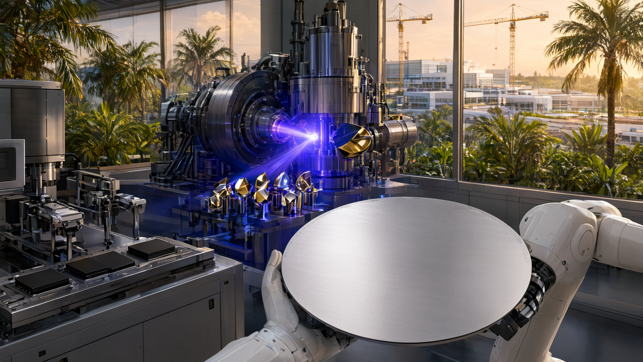
Semiconductor Engineering's weekly roundup reports that fab expansion is accelerating worldwide, with heavy spending on 300mm wafer plants. China is making progress in both memory chips and EUV lithography, the ultra-precise technology behind advanced chips. Teradyne announced a test equipment deal, advanced packaging (3D system-in-package) featured prominently at industry events, optical and 3D-compute startups raised fresh funding, and quantum hardware advanced. For Malaysian readers, the pattern matters most in one place: value in the chip chain is shifting toward packaging and test — Malaysia's core strengths — while geopolitical fragmentation raises both risk and opportunity for local firms.
AI Summary
Semiconductor Engineering's weekly roundup reports that fab expansion is accelerating worldwide, with heavy spending on 300mm wafer plants. China is making progress in both memory chips and EUV lithography, the ultra-precise technology behind advanced chips. Teradyne announced a test equipment deal, advanced packaging (3D system-in-package) featured prominently at industry events, optical and 3D-compute startups raised fresh funding, and quantum hardware advanced. For Malaysian readers, the pattern matters most in one place: value in the chip chain is shifting toward packaging and test — Malaysia's core strengths — while geopolitical fragmentation raises both risk and opportunity for local firms.
Key Takeaways
- Fab expansion is accelerating, and money is flowing into 300mm wafer plants — a read on industry confidence in long-term AI chip demand.
- China is advancing its own memory technology and working toward domestic EUV lithography, deepening the split between two global chip supply chains.
- Teradyne's test deal reflects a real bottleneck: as chips become stacks of multiple dies, testing them is getting harder and more commercially important.
- 3D system-in-package (SiP) is where performance gains now come from — and it moves engineering value into packaging, which is Malaysia's traditional stronghold.
- Optical and 3D-compute startups raised new funding, and quantum hardware advanced — both early-stage bets driven by AI data centre power constraints.
What Happened
Semiconductor Engineering's weekly review collected the industry's main developments in one place. The headline theme is physical buildout: fabrication plants ("fabs," the factories where chips are made) are expanding at an accelerating pace, and spending on 300mm fabs — plants that process large silicon wafers 300 millimetres across, the standard for modern chipmaking — is rising. More fab capacity takes years and billions of dollars to build, so companies only commit when they expect demand far into the future.
China featured twice. Its firms are advancing memory chip capability, and there is continued progress toward domestic EUV — extreme ultraviolet lithography, the printing technology that etches the finest circuit patterns onto chips. EUV machines are currently supplied almost exclusively by ASML of the Netherlands, and export restrictions have blocked their sale to China, which is why China is building its own.
The roundup also covered Teradyne, a major test equipment maker, which announced a deal — a signal that chip test capacity is in demand. Highlights came from SEMICON West, the big semiconductor trade show, and OCP, the Open Compute Project community that shapes data centre hardware. On the technology front, 3D SiP — stacking multiple chip dies into a single package to make systems faster and smaller — drew attention. TSMC, the world's largest contract chipmaker, and ASML both sent signals the industry watches closely for demand and technology direction. Finally, startups working on optical computing (processing and moving data with light) and 3D compute raised fresh funding, and quantum hardware saw further advances.
Why It Matters
Every AI model you use — from ChatGPT to a bank's fraud detection system — runs on physical silicon. When fab spending accelerates, the industry is voting with money that AI compute demand will keep growing for years. That matters beyond chipmakers: it shapes lead times and prices for every electronic product, from factory sensors to servers, and it drives energy demand and investment across Asia. Think of fab spending as a leading indicator, like construction permits for the digital economy.
The China-EUV story is the geopolitical one. If China succeeds in domestic EUV and memory, the world moves from one shared chip supply chain toward two parallel systems — one Western-aligned, one Chinese. That changes sourcing strategy for every multinational and every supplier that feeds them. The timeline is genuinely uncertain; success is not guaranteed, but the direction of travel is clear.
The quiet structural shift is packaging and test. For decades, performance gains came from shrinking transistors, and assembly was the low-margin back end of the industry. With 3D SiP, the package itself becomes the product: how you stack and connect dies now determines speed, power, and reliability. That is why Teradyne's test deal matters too — stacked dies multiply the number of things that can fail, and testing complexity rises accordingly. The back end of the chip chain is becoming the high-value end. That is not my wishful reading; it is what the week's technology headlines — 3D SiP, test deals, SEMICON and OCP focus — are collectively pointing at.
What This Means for Malaysia
Malaysia is one of the world's largest centres for chip assembly, test, and packaging, concentrated in Penang and Kulim. That position exists precisely because packaging and test used to be the commoditised back end. If value now migrates into 3D SiP and complex test — the exact trends in this week's roundup — Malaysia's existing infrastructure, engineers, and multinational relationships become more strategically important, not less. The opportunity is real, but so is the condition: local operations must upgrade from traditional wire-bond assembly to advanced packaging processes and test engineering for stacked dies. Government direction, including the national semiconductor strategy and MDEC's investment attraction work, aligns with this, but the skills gap is where the race is won or lost.
The China angle cuts both ways for Malaysian firms. A second, Chinese-led chip supply chain creates new potential customers for Malaysian packaging and test providers — and new competition, plus compliance complexity if you serve customers on both sides. Malaysian electronics SMEs in the supplier ecosystem should assume export-control rules will keep changing, and structure customer bases so no single region
Sources & References
AIBlog summarises and analyses published information. We do not reproduce full source text. Analysis is editorial and not financial or legal advice.